
Khung bảo vệ EMI RF SMD PCB được đóng dấu chính xác cho các ứng dụng tần số cao
-
Làm nổi bật
Bộ bảo vệ RF PCB được đóng dấu chính xác
,Ống che chắn EMI SMD
,Nắp tấm chắn PCB tần số cao
-
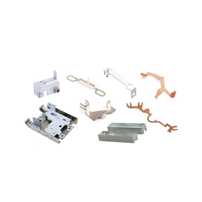
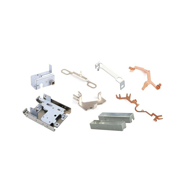
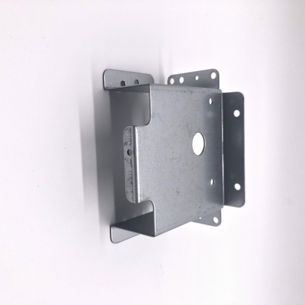
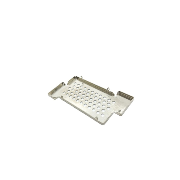
Các sản phẩmTấm chắn bảo vệ PCB EMI PCB RF, tiếp điểm dập, bộ phận kim loại
-
Quá trìnhTấm kim loại bị chế tạo, hàn giập giòn giòn
-
Ứng dụngVỏ bảo vệ PCB EMI PCB RF, Vỏ PCB di động
-
Sức chịu đựng+/- 0,02mm
-
Thiết bịBộ phận dập chính xác
-
Vật liệuHợp kim đồng-niken-kẽm tấm thiếc
-
Chức năngVỏ che chắn
-
Đã sử dụngBảng PCB, vỏ điện thoại di động, máy tính, GPS, đồng hồ, sản phẩm kỹ thuật số và các sản phẩm điện t
-
Bề mặt hoàn thiệningbình thường, mạ thiếc, mạ niken
-
Bưu kiệnTúi platic, hộp phồng rộp, nhấn cuộn hoặc theo yêu cầu của bạn
-
TênKim loại dập tùy chỉnh chính xác SMD PCB RF EMI Shield Cover, Shield Frame
-
cung cấp100000/tháng
-
Nguồn gốcTrung Quốc
-
Hàng hiệuXianheng
-
Chứng nhậnISO 9001:2015 SGS RoHS
-
Số mô hìnhRF-XG-40
-
Tài liệu
-
Số lượng đặt hàng tối thiểu1 PC
-
Giá bánUSD 0.01$-0.5$
-
chi tiết đóng góiHộp gỗ carton
-
Thời gian giao hàng5-8 ngày
-
Điều khoản thanh toánT/T, Western Union, Moneygram
-
Khả năng cung cấp10000 BỘ mỗi tuần
Khung bảo vệ EMI RF SMD PCB được đóng dấu chính xác cho các ứng dụng tần số cao
Chuyển đổi tấm kim loại thành PCB tùy chỉnh RF Shields Đánh dấu kim loại chính xác cho các ứng dụng tần số cao
Mô tảChuyển đổi tấm kim loại thành PCB tùy chỉnh RF Shields Đánh dấu kim loại chính xác cho các ứng dụng tần số cao
Bấm kim loại chính xác là một quy trình sản xuất chuyên biệt biến các tấm kim loại phẳng thành các tấm bảo vệ tần số vô tuyến (RF) được thiết kế tùy chỉnh cho bảng mạch in (PCB).Những tấm chắn này là thành phần quan trọng trong các ứng dụng điện tử tần số cao, như viễn thông, hàng không vũ trụ và thiết bị y tế,khi nhiễu điện từ (EMI) và nhiễu tần số vô tuyến (RFI) phải được giảm thiểu để đảm bảo hiệu suất và độ tin cậy tối ưu.
Vật liệu củaChuyển đổi tấm kim loại thành PCB tùy chỉnh RF Shields Đánh dấu kim loại chính xác cho các ứng dụng tần số cao
| Báo cáo về vật liệu và thử nghiệm | ||
| Kim loại | Nhôm | Nhôm 2024 Nhôm 5052 Nhôm 6061-T6 |
| Nhôm 6063 Nhôm 7075 Nhôm MIC 6 | ||
| Thép không gỉ | SUS303, SUS304, SS316, SS316L | |
| UNS S32304 UNS S32003 UNS S31803 UNS S32205 | ||
| UNS S32760 UNS S32750 UNS S32550 UNS S32707 | ||
| Thép | 12L14 4140 1018 1045 | |
| D2 thép dụng cụ,A36 1008,Alloy42 | ||
| Titanium | Các lớp 1-4 lớp 5 lớp 9 | |
| Đồng | 260, C360, H59, H60, H62, H63, H65, H68, H70 | |
| Đồng | ||
| Phosphor đồng | ||
| Đồng | C932 | |
| Sợi carbon | ||
| PTFE | Polytetrafluoroethylene (PTFE) | |
| Nhựa | Acetal | (Polyoxymethylene (POM)) [Delrin] |
| PEEK | Polycarbonate | |
| Polystyrene | Polyether Ketone | |
| Nhựa nhựa | ||
| ABS | ||
| PVC | ||
| Acrylic | ||
| G-10 Sợi thủy tinh Garolite | ||
| Kết quả cuối cùng | |
| Như máy móc | Biên sắc và đục sẽ được loại bỏ |
| Vụ nổ hạt | Bề mặt của bộ phận được để lại với một bề mặt mịn, mờ |
| Được anodized | Loại II tạo ra một kết thúc chống ăn mòn. Các bộ phận có thể được anodized trong các màu sắc khác nhau, rõ ràng, đen, đỏ và vàng là phổ biến nhất và thường được liên kết với nhôm. |
Loại III dày hơn và tạo ra một lớp chống mòn ngoài khả năng chống ăn mòn | |
| Lớp bột | Đây là một quá trình mà sơn bột được phun lên một bộ phận sau đó được nướng trong lò. |
| Tùy chỉnh | Hãy liên hệ với chúng tôi qua email, Skype, WhatsApp. Chúng tôi sẽ xem xét một quá trình hoàn thiện cho bạn. |
| Các loại khác | |
| Sự khoan dung | +/- 0,005mm |
| Thời gian dẫn đầu | 1-2 tuần cho mẫu, 3-4 tuần cho sản xuất hàng loạt |
| Hình vẽ được chấp nhận | Solid Works, Pro / Engineer, AutoCAD ((DXF, DWG), PDF |
| Điều khoản thanh toán | TT/Paypal/WestUnion |
Ngành công nghiệpChuyển đổi tấm kim loại thành PCB tùy chỉnh RF Shields Đánh dấu kim loại chính xác cho các ứng dụng tần số cao
1Các bộ phận máy bay
2. Phụ tùng ô tô
3Các bộ phận thiết bị
4Các bộ phận y tế
5Các bộ phận hóa chất dầu
6Các phần giáo dục
Đặc điểm củaChuyển đổi tấm kim loại thành PCB tùy chỉnh RF Shields Đánh dấu kim loại chính xác cho các ứng dụng tần số cao
1. Độ chính xác cao
2. Thời gian xử lý ngắn
3. Dễ dàng tùy chỉnh / cá nhân hóa
![]()
Lợi ích của chúng ta
Độ chính xác cao và chính xác:Chấm kim loại chính xác cho phép sản xuất các tấm chắn RF với độ khoan dung cực kỳ chặt chẽ và hình học phức tạp.Giảm thiểu các lỗ hổng và rò rỉ có thể ảnh hưởng đến hiệu quả bảo vệTrong các ứng dụng tần số cao, ngay cả những khiếm khuyết nhỏ cũng có thể dẫn đến sự suy giảm hiệu suất đáng kể, làm cho việc đóng dấu chính xác rất cần thiết.
Hiệu quả chi phí:So với các phương pháp sản xuất khác như CNC gia công hoặc in 3D, kim loại chính xác đóng dấu cung cấp một giải pháp hiệu quả hơn chi phí cho sản xuất khối lượng lớn.quá trình đóng dấu có thể nhanh chóng sản xuất một lượng lớn các tấm chắn RF giống hệt nhau với chi phí đơn vị thấp hơn, làm cho nó lý tưởng cho sản xuất hàng loạt trong các ngành công nghiệp như điện tử tiêu dùng và ô tô.
Hiệu quả vật liệu:Chấm kim loại chính xác tối ưu hóa việc sử dụng vật liệu bằng cách giảm thiểu chất thải trong quá trình sản xuất.Các đốm được thiết kế để tối đa hóa số lượng lá chắn có thể được sản xuất từ một tấm kim loại duy nhất, giảm chi phí vật liệu và tác động môi trường.có thể có lợi trong các ứng dụng mà trọng lượng và không gian là yếu tố quan trọng.
Hiệu suất bảo vệ được cải thiện:Các tấm chắn RF được thiết kế tùy chỉnh được sản xuất thông qua dán kim loại chính xác có thể được điều chỉnh cho các yêu cầu ứng dụng tần số cao cụ thể.Các tấm chắn có thể được thiết kế để cung cấp hiệu quả chắn tối ưu trên một phạm vi tần số rộng, đảm bảo rằng các thành phần điện tử nhạy cảm được bảo vệ khỏi EMI và RFI.làm cho việc đóng dấu chính xác là sự lựa chọn ưa thích cho các ứng dụng hiệu suất cao.
![]()
Câu hỏi thường gặp
Q1: Tôi có thể lấy thông tin về sản phẩm và giá ở đâu?
A1:Gửi cho chúng tôi e-mail yêu cầu, chúng tôi sẽ liên hệ với bạn khi chúng tôi nhận được thư của bạn.
Q2: Tôi có thể lấy mẫu trong bao lâu?
A2: Tùy thuộc vào các mặt hàng cụ thể của bạn, trong vòng 3-7 ngày thường được yêu cầu.
Q3: Những loại thông tin bạn cần cho báo giá?
A3: Xin vui lòng cung cấp bản vẽ sản phẩm theo PDF, và sẽ tốt hơn nếu bạn có thể cung cấp theo STEP hoặc IGS.
Q4: Các điều khoản thanh toán là gì?
A4: Chúng tôi chấp nhận 50% tiền đặt cọc thanh toán, khi hàng hóa được thực hiện, chúng tôi chụp ảnh cho séc của bạn và sau đó bạn trả số dư.
Q5: Bạn là một công ty thương mại hoặc nhà máy?
A5: Chúng tôi là nhà máy trực tiếp với 10 kỹ sư có kinh nghiệm và hơn 650 nhân viên cũng như khoảng khu vực hội thảo 2000 mét vuông.
Q6: Chúng ta sẽ làm gì nếu chúng ta không có bản vẽ?
A6:Vui lòng gửi mẫu của bạn đến nhà máy của chúng tôi, sau đó chúng tôi có thể sao chép hoặc cung cấp cho bạn các giải pháp tốt hơn.CAD hoặc 3D file sẽ được thực hiện cho bạn nếu đặt hàng.
Sản phẩm của chúng tôi được bán trên toàn thế giới. Bạn có thể yên tâm về toàn bộ quá trình sản xuất sản phẩm của chúng tôi.