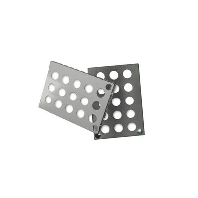
Customized Precision Metal Stamping for EMI RFI Protection in High-Frequency Electronic Devices with Custom PCB RF Shield
-
Highlight
High Frequency PCB RF Shield
,EMI RFI Protection PCB RF Shield
,Customized PCB RF Shield
-
ProductsSMD EMI PCB RF Shield Cover,stamping Contacts, Metal Parts
-
ProcessMetal Sheets Fabrication,Welding Cutting Punching Stamping
-
ApplicationSMD EMI PCB RF Shield Cover,Mobile PCB Cover
-
Tolerance+/-0.02mm
-
EquipmentPrecision Stamping Parts
-
MaterialTin Plate Copper-Nickel-Zinc Alloy
-
FunctionShielding Cover
-
UsedPCB Board,mobile Phones Cover, Computers, GPS, Watches, Digital Products And Other Electronic Products, Prevent Electromagnetic Interference (EMI), On PCB Components And LCM Shield
-
Surface FinishingNormal,tin Plating ,nickel Plating
-
PackagePlatic Bag ,Blister Box ,Tap Reel Or As Your Required
-
NamePrecision Custom Stamping Metal SMD PCB RF EMI Shield Cover, Shield Frame
-
Supply100000/month
-
Place of OriginChina
-
Brand NameXianheng
-
CertificationISO 9001:2015 SGS RoHS
-
Model NumberRF-XG-35
-
Document
-
Minimum Order Quantity1 pcs
-
PriceUSD 0.01$-0.5$
-
Packaging DetailsCarton Wooden case
-
Delivery Time5-8 days
-
Payment TermsT/T, Western Union, MoneyGram
-
Supply Ability10000 SET per week
Customized Precision Metal Stamping for EMI RFI Protection in High-Frequency Electronic Devices with Custom PCB RF Shield

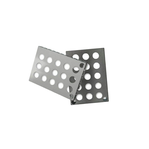
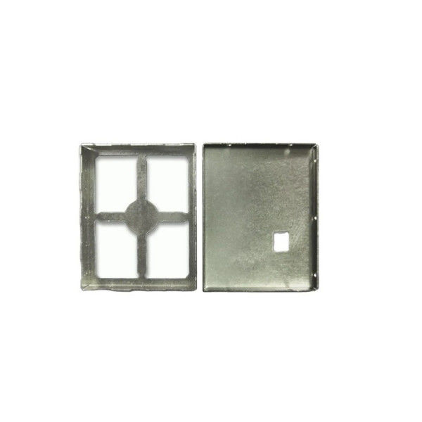
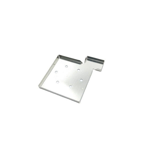
Customized Precision Metal Stamping for EMI RFI Protection in High-Frequency Electronic Devices with Custom PCB RF Shield
Description Of Customized Precision Metal Stamping for EMI RFI Protection in High-Frequency Electronic Devices with Custom PCB RF Shield
Customized precision metal stamping is a specialized manufacturing process tailored to produce high-precision electromagnetic interference (EMI) and radio frequency interference (RFI) shielding solutions for printed circuit boards (PCBs) operating in high-frequency environments (e.g., 5G, Wi-Fi 6E, radar, IoT, and automotive radar systems). This method combines advanced tooling, material selection, and engineering design to create bespoke RF shields that ensure signal integrity, electromagnetic compatibility (EMC), and regulatory compliance while optimizing cost, weight, and assembly efficiency.
Material Of Customized Precision Metal Stamping for EMI RFI Protection in High-Frequency Electronic Devices with Custom PCB RF Shield
| Material and Testing Report | ||
| Metal | Aluminum | Aluminum 2024 Aluminum 5052 Aluminum 6061-T6 |
| Aluminum 6063 Aluminum 7075 Aluminum MIC 6 | ||
| Stainlesss steel | SUS303, SUS304, SS316, SS316L | |
| UNS S32304 UNS S32003 UNS S31803 UNS S32205 | ||
| UNS S32760 UNS S32750 UNS S32550 UNS S32707 UNS S33207 | ||
| Steel | 12L14 4140 1018 1045 12L14 4130 4142 ,O1 tool steel, | |
| D2 tool steel,A36 1008 ,Alloy42 | ||
| Titanium | Grades 1-4 Grade 5 Grade 9 | |
| Brass | 260, C360, H59, H60, H62, H63, H65, H68, H70 | |
| Copper | ||
| Phosphor bronze | ||
| Bronze | C932 | |
| Carbon fiber | ||
| PTFE | Polytetrafluoroethylene (PTFE) | |
| Plastic | Acetal | (Polyoxymethylene (POM)) [Delrin] |
| PEEK | Polycarbonate | |
| Polystyrene | Polyether Ketone | |
| Nylon | ||
| ABS | ||
| PVC | ||
| Acrylic | ||
| G-10 Garolite Fiberglass | ||
| Finish Result | |
| As Machined | Sharp edge and burrs will be removed |
| Bead Blast | The part surface is left with a smooth, matte appearance |
| Anodized | Type II creates a corrosion-resistant finish. Parts can be anodized in different colors—clear, black, red, and gold are most common—and is usually associated with aluminum. |
Type III is thicker and creates a wear-resistant layer in addition to the corrosion resistance | |
| Powder Coat | This is a process where powdered paint is sprayed onto a part which is then baked in an oven. |
| Customized | Cotact us via email, skype, whatsapp. We will look into a finishing process for you. |
| Others | |
| Tolerance | +/-0.005mm |
| Lead Time | 1-2 weeks for samples, 3-4 weeks for mass production |
| Drawing Accepted | Solid Works, Pro/Engineer, AutoCAD(DXF, DWG), PDF |
| Payment Terms | TT/Paypal/WestUnion |
Industries Of Customized Precision Metal Stamping for EMI RFI Protection in High-Frequency Electronic Devices with Custom PCB RF Shield
1. Aircraft parts
2. Automobile parts
3. Fixture parts
4. Medical parts
5. Petro chemical parts
6. Education parts
Features Of High Quality RF Shield
1. High precision
2. Short processing time
3. Easier customized/personalized
![]()
Our Advantages
1. Optimized Performance in High-Frequency Environments
Reduced Crosstalk & Noise: Custom shields isolate sensitive RF components (e.g., oscillators, mixers, amplifiers) from interference, improving signal-to-noise ratio (SNR) and bit error rate (BER).
Frequency-Specific Shielding: Tailored designs (e.g., slotted or perforated shields) can balance shielding effectiveness (SE) with ventilation needs for thermal management in compact devices.
2. Cost Efficiency & Scalability
Low Tooling Costs: Stamping dies are reusable and cost-effective compared to CNC machining or photochemical etching, especially for mid-to-high volumes (10,000+ units).
Material Efficiency: Advanced nesting algorithms minimize scrap, reducing material costs by 20–40% compared to laser-cut or folded shields.
3. Accelerated Time-to-Market with Rapid Prototyping
Fast Design Iterations: In-house tooling and digital twin simulations enable 24–72-hour prototype delivery, allowing quick EMC testing and design refinement.
Seamless PCB Integration: Shields are designed for automated pick-and-place assembly, eliminating manual soldering or adhesive bonding steps and reducing labor costs by up to 50%.
![]()
FAQ
Q1: Where can I get product & price information?
A1:Send us inquiry e-mail, we will contact you as we receive your mail.
Q2: How long can I get the sample?
A2:Depends on your specific items, within 3-7 days is required generally.
Q3: What kinds of information you need for quote?
A3:Kindly please provide the product drawing in PDF, and will be better you can provide in STEP or IGS.
Q4: What are the payment terms?
A4: We accept 50% as payment deposit, when the goods is done, we take photos for your check and you then pay the balance.
Q5: Are you a trading company or factory?
A5:We are direct factory with 10 experienced engineers and more than 650 employees as well approximate 2,000 square ft. workshop area.
Q6: What shall we do if we do not have drawings?
A6:Please send your sample to our factory, then we can copy or provide you better solutions. Please send us pictures or drafts with dimensions (Length, Hight, Width), CAD or 3D file will be made for you if placed order.
Our products are sold all over the world, you can rest assured.