Precision Metal Stamping for Customized PCB RF Shields The Optimal Solution for High-Frequency EMI RFI Protection
-
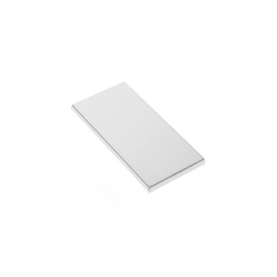
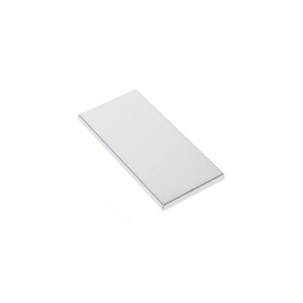
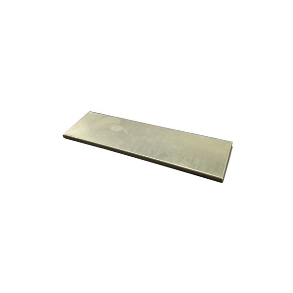
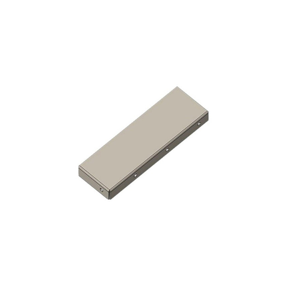
ProductsSMD EMI PCB RF Shield Cover,stamping Contacts, Metal Parts
-
ProcessMetal Sheets Fabrication,Welding Cutting Punching Stamping
-
ApplicationSMD EMI PCB RF Shield Cover,Mobile PCB Cover
-
Tolerance+/-0.02mm
-
EquipmentPrecision Stamping Parts
-
MaterialTin Plate Copper-Nickel-Zinc Alloy
-
FunctionShielding Cover
-
UsedPCB Board,mobile Phones Cover, Computers, GPS, Watches, Digital Products And Other Electronic Products, Prevent Electromagnetic Interference (EMI), On PCB Components And LCM Shield
-
Surface FinishingNormal,tin Plating ,nickel Plating
-
PackagePlatic Bag ,Blister Box ,Tap Reel Or As Your Required
-
NamePrecision Custom Stamping Metal SMD PCB RF EMI Shield Cover, Shield Frame
-
Supply100000/month
-
Place of OriginChina
-
Brand NameXianheng
-
CertificationISO 9001:2015 SGS RoHS
-
Model NumberRF-XG-39
-
Document
-
Minimum Order Quantity1 pcs
-
PriceUSD 0.01$-0.5$
-
Packaging DetailsCarton Wooden case
-
Delivery Time5-8 days
-
Payment TermsT/T, Western Union, MoneyGram
-
Supply Ability10000 SET per week
Precision Metal Stamping for Customized PCB RF Shields The Optimal Solution for High-Frequency EMI RFI Protection

Precision Metal Stamping for Customized PCB RF Shields The Optimal Solution for High-Frequency EMI RFI Protection
Description Of Precision Metal Stamping for Customized PCB RF Shields The Optimal Solution for High-Frequency EMI RFI Protection
Precision metal stamping is a high-precision manufacturing process that transforms flat metal sheets (e.g., steel, aluminum, nickel silver, or copper alloys) into custom-designed PCB RF shields using specialized dies and high-speed presses. This method is ideal for high-frequency electronic applications (e.g., 5G, Wi-Fi 6/7, automotive radar, and medical devices) where tight tolerances, cost efficiency, and reliable EMI/RFI shielding are critical.
Material Of Precision Metal Stamping for Customized PCB RF Shields The Optimal Solution for High-Frequency EMI RFI Protection
| Material and Testing Report | ||
| Metal | Aluminum | Aluminum 2024 Aluminum 5052 Aluminum 6061-T6 |
| Aluminum 6063 Aluminum 7075 Aluminum MIC 6 | ||
| Stainlesss steel | SUS303, SUS304, SS316, SS316L | |
| UNS S32304 UNS S32003 UNS S31803 UNS S32205 | ||
| UNS S32760 UNS S32750 UNS S32550 UNS S32707 UNS S33207 | ||
| Steel | 12L14 4140 1018 1045 12L14 4130 4142 ,O1 tool steel, | |
| D2 tool steel,A36 1008 ,Alloy42 | ||
| Titanium | Grades 1-4 Grade 5 Grade 9 | |
| Brass | 260, C360, H59, H60, H62, H63, H65, H68, H70 | |
| Copper | ||
| Phosphor bronze | ||
| Bronze | C932 | |
| Carbon fiber | ||
| PTFE | Polytetrafluoroethylene (PTFE) | |
| Plastic | Acetal | (Polyoxymethylene (POM)) [Delrin] |
| PEEK | Polycarbonate | |
| Polystyrene | Polyether Ketone | |
| Nylon | ||
| ABS | ||
| PVC | ||
| Acrylic | ||
| G-10 Garolite Fiberglass | ||
| Finish Result | |
| As Machined | Sharp edge and burrs will be removed |
| Bead Blast | The part surface is left with a smooth, matte appearance |
| Anodized | Type II creates a corrosion-resistant finish. Parts can be anodized in different colors—clear, black, red, and gold are most common—and is usually associated with aluminum. |
Type III is thicker and creates a wear-resistant layer in addition to the corrosion resistance | |
| Powder Coat | This is a process where powdered paint is sprayed onto a part which is then baked in an oven. |
| Customized | Cotact us via email, skype, whatsapp. We will look into a finishing process for you. |
| Others | |
| Tolerance | +/-0.005mm |
| Lead Time | 1-2 weeks for samples, 3-4 weeks for mass production |
| Drawing Accepted | Solid Works, Pro/Engineer, AutoCAD(DXF, DWG), PDF |
| Payment Terms | TT/Paypal/WestUnion |
Industries Of Precision Metal Stamping for Customized PCB RF Shields The Optimal Solution for High-Frequency EMI RFI Protection
1. Aircraft parts
2. Automobile parts
3. Fixture parts
4. Medical parts
5. Petro chemical parts
6. Education parts
Features Of Precision Metal Stamping for Customized PCB RF Shields The Optimal Solution for High-Frequency EMI RFI Protection
1. High precision
2. Short processing time
3. Easier customized/personalized
![]()
Our Advantages
Unmatched Precision & Design Flexibility
Stamping achieves tolerances as tight as ±0.01mm, enabling perfect alignment with high-density PCB components.
Custom shapes, cutouts, and features (e.g., EMI gaskets, heat sinks, or RF filtering windows) can be integrated without compromising shielding effectiveness.
Cost-Effective High-Volume Production
Unlike CNC machining or laser cutting, stamping is a high-speed, low-waste process, reducing per-unit costs for large-scale orders.
Tooling costs are lower than injection molding or die-casting, making it ideal for both prototyping and mass production.
Superior EMI/RFI Shielding Performance
Stamped metal shields provide consistent conductivity (e.g., nickel silver offers excellent attenuation up to 60+ dB at GHz frequencies).
The Faraday cage effect is maximized due to seamless contact with PCB ground planes, preventing signal leakage and crosstalk.
Durability & Reliability in Demanding Environments
Stamped shields are mechanically robust, withstanding vibration, thermal cycling, and mechanical stress better than alternative methods.
They can be plated or coated (e.g., electroplating, anodizing, or passivation) for enhanced corrosion resistance and solderability during PCB assembly.
![]()
FAQ
Q1: Where can I get product & price information?
A1:Send us inquiry e-mail, we will contact you as we receive your mail.
Q2: How long can I get the sample?
A2:Depends on your specific items, within 3-7 days is required generally.
Q3: What kinds of information you need for quote?
A3:Kindly please provide the product drawing in PDF, and will be better you can provide in STEP or IGS.
Q4: What are the payment terms?
A4: We accept 50% as payment deposit, when the goods is done, we take photos for your check and you then pay the balance.
Q5: Are you a trading company or factory?
A5:We are direct factory with 10 experienced engineers and more than 650 employees as well approximate 2,000 square ft. workshop area.
Q6: What shall we do if we do not have drawings?
A6:Please send your sample to our factory, then we can copy or provide you better solutions. Please send us pictures or drafts with dimensions (Length, Hight, Width), CAD or 3D file will be made for you if placed order.
Our products are sold all over the world, you can rest assured.